ICEINSPACE

|
One Off Printed Circuit Board Making at Home
Submitted: Tuesday, 12th January 2010 by Steve B
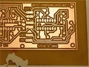
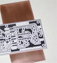
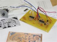
This article includes details about the success I have had making Printed Circuit Boards (PCBs) at home. Over probably 25-30 years I have made my own PCBs from projects in EA and Silicon Chip magazines, producing one-offs. I have tried just about all methods, the Positive resist photo-art, Negative Resist, Direct artwork and etch (decals and pen), but I never did have much success with Toner Transfer method. Many good articles describe it. Here are two good ones: http://gilmore2.chem.northwestern.ed...garbz2_prj.php Anyway, my attempts years ago with Toner Transfer method always were touch and go. I could never rely on fine details to reproduce. Surface Mount Devices a definite no-go. Even DIL ICs sometimes had tracks joined and fine lines with pinholes etc. Well my need to produce a quick, accurate one-off a few weeks back made me re-try the TT method. The success all comes down to the choice of printer paper as the above links stress several times. I thought I'd be smart and try normal A4 paper. The result was pinholes, tracks lifted, Failure! I then tried tracer paper A4: The same result. Then I tried some good quality photo printer paper for bubblejets. I used Kodak Picture Paper Cat # 835 0613 on a HP laserjet (toner) printer. Outstanding success! The artwork was reproduced intact and it etched the best I have EVER etched an artwork. That includes some of my best stuff done with the reliable Riston process. I am so impressed with how faithfully it worked that I am confident it would work with dual layer stuff and SMD. I tried several re-tries so that I could demonstrate it wasn't a fluke. The links above seem to infer that the method is not really for a fine detailed project but I now have every confidence that it is.
A few notes about the Toner Transfer Method My aim is not to duplicate the above links but just record the method that worked for me because it was so successful. It may be of some help to people making quick, repeatable PCBs like I do occasionally. Ok, so here is a detailed description of how this process works. Again, this process makes high detail artwork survive the etch process faithfully, and therefore, is a perfectly viable cheap method.
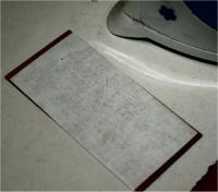
4. The PCB is very hot now and I dropped it into the kitchen sink filled with warm water (below). 5. After very carefully rolling the printout layer with your thumb under water you can remove all of the paper remnants until the artwork (toner) is left intact. In my case it takes on a greyish appearance. Carefully inspect you have 'rolled' all of the paper off, especially between IC pads etc because if you leave ANY paper behind at this stage the etchant will also leave that copper behind.
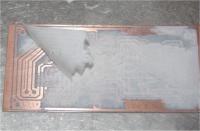
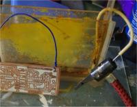
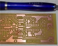
5. Etching (below left) shows my small etching tank, fed with regulated compressed air to speed up the process. Pre-heating Ferric Chloride to above 30-40°C also speeds it up. Be very careful with FeCl because it is highly corrosive. Etching is complete in about 2-3 mins with good fresh Ferric Chloride. 6. All done! (below right). A completed board, washed down and ready to drill.
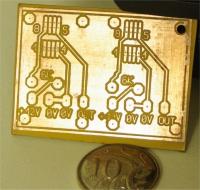
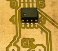
Below are some shots of some SMD boards I made. A rough LM335 test board. The pattern shows an SO8 surface mount spacing. Again, very fine line reproduction. Impressed!
To summarise, this method really works! The best part about it is when I can go from having the design on screen, to a printout, to etch, then sitting in my hands ready to solder in about ten minutes. The bottom line is that it works reliably with a minimum of variables that might mean success or failure. You’ve gotta be happy with that! :)
Article by Steve B (kinetic). Discuss this Article on the IceInSpace Forum.  |
|
||||||||||||||||||||||||||||||||||||||||||||||||||